
PCB Layout Service
With over 17 years of experience in PCB fabrication and extensive development in EasyEDA PCB design software, we can help you in swiftly transitioning from concept to production, accelerating your product's time to market.


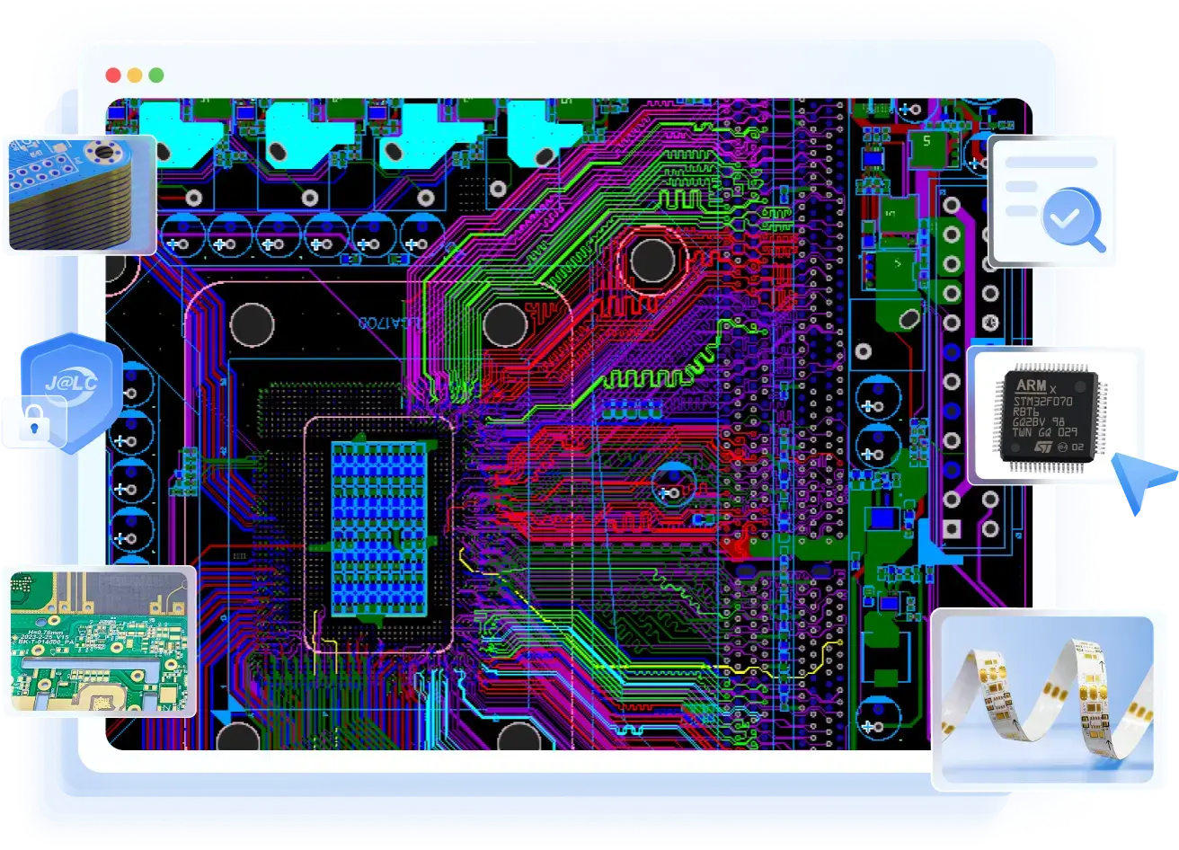
Integrated With Manufacturing
As a one-stop solution provider, we offer seamless integration with manufacturing, from PCB layout to PCB Production - PCB Assembly - Components Sourcing -3D Printing - CNC Machining.
Professional & Complex Design
We provide experienced engineer consulting, impedance calculation, PCB stack-up and DFM check. PCB designs involving high-frequency, high-speed, FPC or high-power etc.
Faster Turnaround Time
Utilize validated modules to improve design efficiency and reduce lead times. With our in-house production and layout services, we can deliver complex designs more quickly.
Cost Optimization
As a PCB manufacturer, we have the expertise to minimize production costs, while ensuring that our PCBs meet the highest standards for performance and manufacturability.
CAPABILITIES AND SERVICES
 PCB Layout Design Up to 50 Layers 0.3mm BGA Pin Spacing 60Ghz High Frequencies Stack-up Design Rigid, Flex, HDI, High-speed, Power boards 100,000 + PIN 2.4mil Trace Width/Spacing Controlled Impedance DFM Check
Bring Your Boards To Life
- Upload Schematic to Get a quote
- JLCPCB Review and Quotation
- Customer Make Payment
- Evaluation and Confirmation of Plan
- Design Start

- Layer Stack-up Design
- Design Rule Setting
- Component Placement Design
- Confirmation and Optimization
- Fanout
- Fanout Optimization
- PCB Routing
- Equal-length Adjustment
- Routing Optimization
- DRC Check
- Routing Confirmation
- Silkscreen Adjustment
- Data Output
- Customer Final Confirmation
- Production Debugging
- Archiving Projects
- Finish

Request a Circuit Board Layout Quote!