01
Free Review & Quotation
3 Hours- ✓ Submit schematic, requirements, and other necessary documents
- ✓ Engineers evaluate feasibility and quotation


Feature | Capability |
|---|
PCB Types | Rigid, Flex, HDI, RF, Power |
Layers | Up to 50-layer design (32-layer manufacturing support) |
Pin Count | 100,000+ pins |
BGA | Down to 0.3mm pitch |
Trace Width/Spacing | Min 2.4 mil (0.06mm) |
High-Speed Design | Multi-GHz digital & RF support(Up to 60 GHz) |
Impedance Control | Full stack-up + impedance matching |
DFM Analysis | Manufacturing risk optimization |
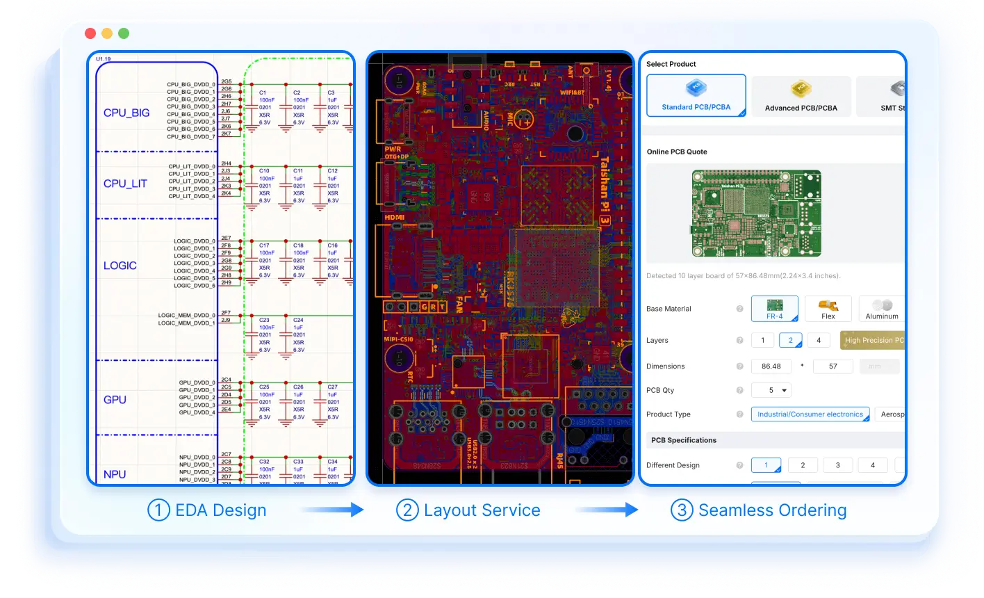
Software Support | EasyEDA · KiCad 8/9/10 · Altium Designer · Cadence Allegro · OrCAD · PADS |
Our services are ideal for:

We provide PCB layout service across multiple industries:
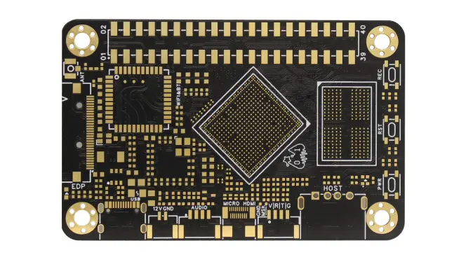
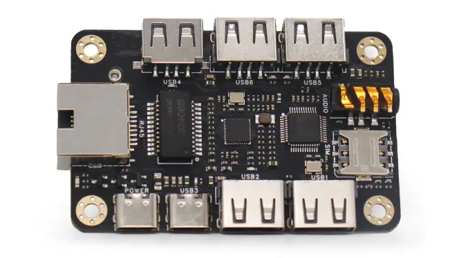
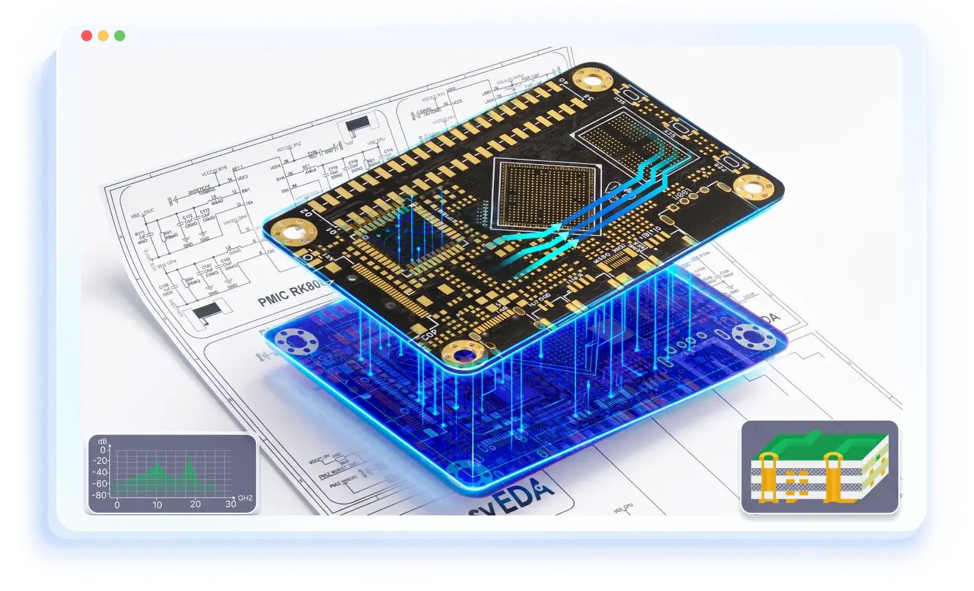
PCB layout is the process of placing components and routing electrical connections on a printed circuit board, transforming a schematic into a manufacturable design. Unlike schematic design — which focuses on circuit logic and functionality — PCB layout focuses on physical implementation, signal integrity, and manufacturability.
Explore best practices, design tips, and engineering insights on our blog to help improve your PCB layout design quality and manufacturability.